Contact us
Contact: Miss Wei +86-18002932564
Phone: +86-769-85168706
Fax: +86-769-85168706
E-mail: 2573495894@qq.com
QQ: 2573495894
Address: No.84, Xinsan Road, Xin'an Avenue, Fanshen Village, Ludong Community, Humen Town, Dongguan City
Schematic diagram of circuit design for eight digit dip switch
2018-12-09
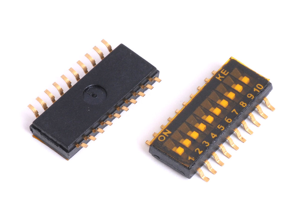
A dip switch is equivalent to a switch quantity. When turned on, it means it is turned on, and when turned off, it means it is turned off. In digital circuits, it is commonly used for binary inputs such as 0 and 1. The minimum system board uses an eight digit dip switch as one byte input. When turned on, it is equivalent to inputting "1", and the default input is "0".
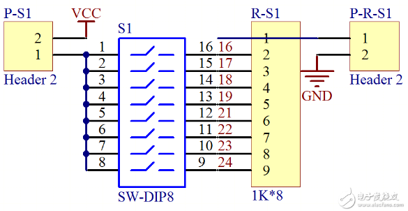
Schematic Design of Eight Position DIP Switch Circuit
Overall circuit schematic diagram of minimum system circuit design
The circuit schematic designed using Aluminum software includes clock circuit, reset circuit, power circuit, JATG circuit, PROM configuration circuit, display module circuit, switch circuit, and various interface circuits for the FPGA minimum system board.
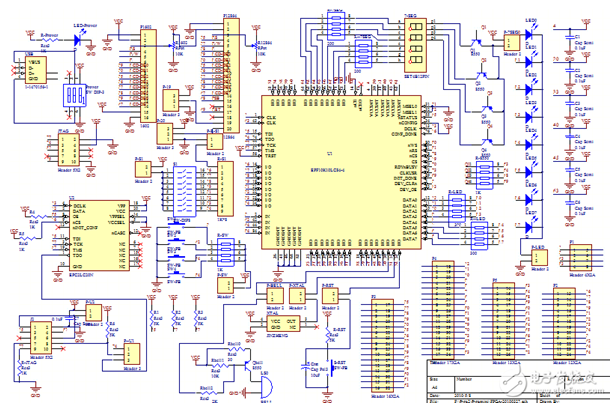
Overall circuit schematic diagram of minimum system circuit design
The application areas of dip switch products have expanded from communication to a wide range of fields such as consumer electronics, automotive electronics, industrial control, testing and measurement. Applying relatively mature technologies to specific fields such as communication, video, information processing, etc. to develop products that meet industry needs and can be accepted by industry customers is mainly a combination of FPGA technology and professional technology. In addition, there are interface issues with professional customers. Product design also includes professional tool products and civilian products, with the former focusing on performance and the latter on price sensitive product design with the main goal of achieving product functionality, FPGA technology is an implementation method in this field. FPGA has the characteristics of interface, control, functional IP, embedded CPU, etc. It has the conditions to realize a system product design with simple structure, high degree of solidification, and comprehensive functions. It will be the most widely used market for FPGA technology application, with great explosive demand space. Product design requires high technical personnel and the journey is also relatively long. However, the entire industry is currently in the state of forming a "debut team". As long as you join, the future is bright. Product design is a career development direction positioning, which cannot be achieved simply by a hobby! The field of product design will create a large number of enterprises and entrepreneurs, which is a development hotspot and opportunity.